研究内容 / Research
酸素と亜鉛の化合物である酸化亜鉛(ZnO)は、化粧品や医薬品に利用され、私たちの生活に身近な材料です。ZnOのバンドギャップは直接遷移型で、その大きさは3.37 eVであり、およそ370 nmの長波長紫外線UVAに相当することから、高効率紫外線発光素子(UV-LED)やUV受光素子(UVセンサ)材料として期待されています。私たちはZnO単結晶の育成およびZnO単結晶基板を用いたZnO系光デバイスの研究・開発に取り組んでいます。
Zinc oxide (ZnO), a compound of oxygen and zinc, is a familiar material used in cosmetics and pharmaceuticals. The band gap of ZnO is a direct transition type, and its size is 3.37 eV, which is equivalent to long-wavelength UVA of about 370 nm. Therefore, ZnO is expected to be useful as a highly efficient UV light-emitting device (UV LED) or UV light-receiving device (UV sensor) material.
We are engaged in the growth of ZnO single crystals and research and development of ZnO-based optical devices using ZnO single crystal substrates.
1.水熱合成法によるZnO単結晶の育成/Growth of a ZnO single crystal by the hydrothermal method
ZnO単結晶の育成にはいくつかの方法がありますが、最も品質が高く大量生産に適した方法が「水熱合成法」です。この方法で大量生産されている結晶の代表例は「人工水晶」です。
図1は水熱合成炉の断面模式図です。オートクレーブの内部に不純物の混入を防ぐためにライナーを設置し、この中でZnO単結晶を育成します。ライナーの下部(溶解領域)に原料となるZnO焼結体を入れ、ライナーの上部(育成領域)にはZnOの種結晶を吊るし、鉱剤となる水酸化カリウム、水酸化リチウム、純水を加えます。溶解領域と結晶育成領域の間には穴の開いたバッフル板が置かれています。オートクレーブとライナーの間には純水が入れられており、高圧高温でもライナーに無理な圧力がかからないようになっています。
通常、300~400℃、30~80 MPaで数か月間育成します。溶解領域よりも結晶育成領域の温度をやや低くすることによって対流を生じさせ、種結晶上にZnO結晶が育成していきます。
There are several methods for growing ZnO single crystals, but the method that produces crystals with the highest quality and suitable for mass production is the "hydrothermal method". A typical of crystals mass-produced by this method in an "artificial crystal".
Fig. 1 is a schematic cross-sectional view of a hydrothermal autoclave. A liner is installed in the autoclave, and a ZnO single crystal is grown in the liner. This liner prevents impurities from getting into the ZnO crystal. ZnO ceramics is put in the lower part of the liner (dissolution region), and the ZnO seed crystal is hung in the upper part of the liner (growth region). KOH, LiOH and deionized water are then added as mineralizers. A baffle plate with holes is placed between the melting area and the growing area. Deionized water is put between the autoclave and the liner so that liner is not subjected to excessive pressure even at high pressure and high temperature. Normally, crystals are grown at temperature of 300 to 400℃ and pressure of 30 to 80 Mpa for several manths. By making the temperature in the growth region slightly lower than the temperature in the melting region, convection is generated and ZnO crystals grown on the seed crystal.
Fig. 2shows the grown ZnO single crystal and Fig. 3 shows the ZnO single crystal substrate.

Fig.1 Schematic cross-sectional view of a hydrothermal autoclave

Fig.2 Grown ZnO single crystal
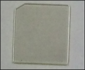
Fig.3 ZnO single crystal substrate
(10 mm×10 mm×0.5 mm)
2.ZnO-UVセンサ/ZnO-UV sensor
本研究室ではZnO単結晶基板のZn面を用いた光導電型UVセンサを開発しています。光導電型は、半導体に入射した光によってキャリアが発生し、導電率が増加する光導電特性を利用するものです。光導電型は構造が非常に簡単で高感度(103 A/W)という特徴があります。
図4は光導電型ZnO-UVセンサの構造図です。電極間にUV光が照射されると光電流が発生し、UVセンサとして動作します。図5は実際に作製した光導電型ZnO-UVセンサになります。このセンサを用いて屋外の太陽光による強いUV光から室内の蛍光灯による弱いUV光まで測定可能なことを確認しています。現在、実用化を目指して応答速度の改善を試みています。
We are also developing a photoconductive UV sensor using the Zn face of a ZnO single crystal substrate. The photoconductive type utilizes the photoconductive property that carriers are generated by light incident on the semiconductor and the conductivity increases. The photoconductive type has a very simple structure and is characterized by high sensitivity (103 A/W).
Fig. 4 shows the structure of the photoconductive type ZnO-UV sensor. When UV light is irradiated between the electrodes, a photocurrent is generated and it operates as a UV sensor. Fig. 5 shows the photoconductive type ZnO-UV sensor.

Fig.4 Structure of the photoconductive type ZnO-UV sensor

Fig.5 Photoconductive type ZnO-UV sensor
3.放射線検出器/Radiation detector
ZnO-UVセンサとYAP:Ceシンチレータを組み合わせた放射線検出器の研究も行っています。YAP:Ce(Ce doped Yttrium Aluminum Perovskite)は放射線を照射するとそのエネルギーを吸収して紫外線を発光する材料です。
図6はZnO-UVセンサの光導電スペクトルとYAP:Ceシンチレータの発光スペクトルを重ねたグラフです。ZnO-UVセンサのピーク光電流とYAP:Ceシンチレータの発光ピークがよく一致していることが分かります。図7はZnO-UVセンサとYAP:Ceシンチレータを組み合わせた放射線検出器の構造図です。YAP:Ceシンチレータに放射線(X線)が入射するとUV光が生じます。このUV光をZnO-UVセンサが受光することで放射線検出器として動作します。
すでにX線を用いた実験を行い、X線に対して動作することを確認しています。現在はYAP:Ceシンチレータの薄膜化も試みています。
We are also studying radiation detectors in which the combination of a ZnO-UV sensor and a YAP:Ce scintillator is used. YAP:Ce (Ce-doped yttrium aluminum perovskite) is a material that absorbs the energy of irradiated radiation and emits ultraviolet light.
Fig. 6 shows a graph in which the photoconductivity spectrum of the ZnO-UV sensor and the emission spectrum of the YAP:Ce scintillator are superimposed. It can be seen that the peak photocurrent of the ZnO-UV sensor and the emission peak of the YAP:Ce scintillator are in good agreement.
Fig. 7 is a structural drawing of a radiation detector in which the combination of a ZnO-UV sensor and a YAP:Ce scintillator is used. UV light is generated when radiation (X-rays) enters the YAP:Ce scintillator. The ZnO-UV sensor receives this UV light and operates as a radiation detector. We have already conducted experiments using X-rays and confirmed that it works with X-rays.
Currently, we are also trying to make the YAP:Ce scintillator tinner.

Fig.6 Photoconductivity spectrum of the ZnO-UV sensor and emission spectrum of the YAP:Ce scintillator
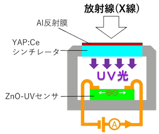
Fig.7 Structural drawing of a radiation detector